We created the first microchips for deep learning — tensor processing units (TPUs). Our first silicon came back from foundry in 2011/2012. The video above shows us opening up our first wafer from TSMC. According to Google Gemini, Google started their TPU project in late 2013, about 4-6 months after I gave the talk there, and completed their first tape-out in silicon about a year and a half later in 2015.
I was the Founder, Chief Scientist, and CEO of Lyric Semiconductor, Inc. which grew out of my PhD work at MIT and Mitsubishi Electric Research Labs (MERL) in Cambridge, MA.
We developed the world’s first deep learning processing units for machine learning, providing huge efficiencies in Joules per Operation wins for deep learning (1,000x – 10,000x). On a range of image processing and signal processing benchmarks, we demonstrated 10x more operations per second (GOPS) and 100x lower power (Joules per operation) compared to the leading Nvidia GPU of the time. Compared to the leading CPU of the time (Intel Core i7) we demonstrated 100x more OPS and 10x lower Joules/operation.
We were acquired by ADI, and our technology incorporated into wireless infrastructure, medical devices, self-driving cars, mobile devices, and other applications.
Published patents include processor architecture1 2, separate model weights memory and memory bus3, factor/tensor operators4, the software framework for developing model architectures5, compiler for going from model to the processor6, I/O7, application in a signal processing pipeline8, methods for deciding which neurons to update9. We used the terms “factor” and “tensors” interchangeably10. We have requested to have the DARPA final report released.
There was also significant press coverage in EE Times, 11, MIT Press 12, MIT Technology Review13, New York Times14, PC World15, eWeek16, The Register17.
In 2010, our processor architecture anticipated the major features of today’s deep learning microchips (tensor processors), and anticipated at least one key feature that as of 2025 to my knowledge has still not been implemented in any commercial deep learning processor architecture:
- We added a third route to memory — for model weights — when the traditional von Neumann computer architecture had always had only two.
Historically, processors had transistors for performing computations located in one area of the chip and, in a separate area, transistors for storing bits – the computer memory. This architecture resembles how neighborhoods can be laid out with a concentrated shopping area with stores where you go to get stuff — like going to get data from memory, and a separate residential area where you process the stuff you buy — bring it home and turn it into something else — the outputs of your life.
On a chip, there are wires leading from the processing area to the memory area to tell the memory area what data we want to recall, and then routes back for that data to flow from the memory to the processor. These routes literally look like little multi-lane highways if you look at them under a microscope.
Until we created our new deep learning processors, the standard computer architecture had two major wire highways — known as “memory buses”. The first bus was for accessing the program memory – the operations that the processor should perform. The second bus was for looking up data — each operation in a program comes with the memory addresses of the data that it plans to operate on.
To these traditional two memory buses (for accessing program memory and data memory), we added a third memory bus – for model weights. Powering the (long) wires that access memory turns out to dominate the energy consumption of processors. This will be the case, as long as we continue to use methods for printing transistors and wires onto semiconductor wafers (lithography) that work the best when we have large, specialized memory areas with highly repetitious, grid-like patterns.
To access our model weights memory, it turned out that we could actually design a much more efficient bus by specializing it for the job. In our design, we took advantage of the fact that our weights would be accessed in parallel for each tensor operation in our deep learning network, and that clumps of weights would be accessed in an orderly way as computations progressed through the deep learning model. - We created a specialized compiler and programming language to take advantage of a deep learning processor, specialized for designing models and compiling them onto our chips. Dimple, “an open-source software tool for probabilistic modeling, inference, and learning” anticipated and helped provide a foundation for the creation of TensorFlow and PyTorch. It was used by Kevin Murphy’s team at Google to create the first version of Google Knowledge Graph.18
- We created the first on-chip weight quantization. In 2009 – 20120, when Hinton et. al. were first experimenting with quantization of neural weights, we had already run massive simulation studies ($300,000 cloud simulations were unheard of at the time) to determine the minimum number of bits needed to represent weights and activations. We learned that weights could always be represented by very compact 8-bit numbers or 2-bit numbers, and took advantage of this in our processing and bus designs.
- [Still novel in 2025?] We strided past zero weights. Many weights in a model learn to be very nearly zero, but a zero weight multiplied by any activation, simply returns zero. A multiply by zero then adds nothing (literally) to the rest of the model computations that come afterwards. So we created a special “striding” unit that could know or predict in advance which weights would be zero and completely skip accessing them and multiplying by them. Part of the reason we could do this was because we designed “a priori” constraints into our models that led to the non-zero weights being distributed in somewhat predictable ways across the model. Predicting where the non-zero weights would be in the processor turned out to be far less expensive in Joules than accessing and multiplying by a group of weights that turn out to be zero. Fifteen years later in 2025, to my knowledge, striding across near-zero weights is still a novel feature.
I gave a Google Tech Talk on July 9, 2013 presenting our benchmark results. This was the outline of the talk. I focused the talk on ML/AI applications that would have value within Android phones, including gesture recognition, speech recognition, and wireless receivers:
The benchmark results in the chart below show that
- Compared to the best NVidia GPU of the time (GeForce GTX 780), our processor (GP5) consumed 10,000x less power while also providing an output in 10x less time.
- Compared to the best CPUs of the time (Intel Core i7), GP5 consumed 100x less power and provided an output 100x faster.
- Compared to ARM cores which are designed for low power in mobile devices, GP5 consumed 100x less power, and provided an output 10,000x faster.
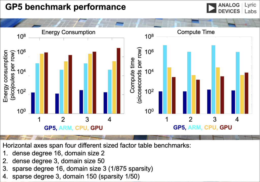
We called our processor the General-Purpose Programmable Parallel Probability Processor (GP5).
The “tensor” in a Tensor Processing Unit (TPU), refers to the structure of the deep learning model and the structure of the operations that need to be performed. The words “tensor” in mathematics and “factor” in connectionist deep learning models were used interchangeably at the time. Google’s tensor processing units (TPUs) and our Probability Processors perform multiplies, adds, and other operations on logits. A semi-ring defines the algebraic structure over which tensor contractions (matrix multiplies, convolutions) execute.
Arguably the most novel and important aspect of this new era of computing is that we are specializing a processor not just for any tensor operations, but specifically for a deep learning model with weights and activations. Instead of operating on bits, such a processor is specialized to operate on logit values (approximate log probabilities). We therefore called our chip a General-Purpose Programmable Parallel Probability Processor (GP5). We even had an analog version of the same processor where the logits were represented by analog electrical currents.
The fascinating thing is that pulling together all of the innovations we combined in these chips, we saw approximately four orders of magnitude benefits to our deep learning processors versus state-of-the-art GPUs. It seems surprising that for example, Google, only publicly claims a 50x and that NVidia has not implemented some of the key features such as dedicated memory access for neural weights in their GPUs.
Is it possible that today in 2026, there are still orders of magnitude in chip architecture power benefits that are not commercially available?
- Programmable Probability Processing, Bernstein, Jeffrey and Vigoda, Benjamin, Analog Devices, Inc., US Patent 9,626,624 B2, issued April 18, 2017. ↩︎
- Belief Propagation Processor (PDF), Reynolds, David and Vigoda, Benjamin, Mitsubishi Electric Research Laboratories / Analog Devices, Inc., US Patent 8,799,346 B2, issued August 5, 2014. ↩︎
- Belief Propagation Processor, Reynolds, David and Vigoda, Benjamin, Mitsubishi Electric Research Laboratories / Analog Devices, Inc., US Patent 8,799,346 B2, issued August 5, 2014. ↩︎
- Belief Propagation Processor, Reynolds, David and Vigoda, Benjamin, Mitsubishi Electric Research Laboratories / Analog Devices, Inc., US Patent 8,799,346 B2, issued August 5, 2014. ↩︎
- Implementation of Factor Graphs, Hershey, Shawn and Vigoda, Benjamin, Lyric Semiconductor, Inc. / Analog Devices, Inc., US Patent Application 20120159408 A1, published June 21, 2012. ↩︎
- Analog Computation Using Numerical Representations with Uncertainty, Vigoda, Benjamin and Bradley, William and Hershey, Shawn and Bernstein, Jeffrey, Lyric Semiconductor, Inc. / Analog Devices, Inc., US Patent 8,458,114 B2, issued June 4, 2013. ↩︎
- Signal Mapping, Vigoda, Benjamin and Bernstein, Jeffrey and Alexeyev, Alexander and Venuti, Jeffrey, Lyric Semiconductor, Inc. / Analog Devices, Inc., published November 4, 2010. US Patent Application 20100281089 A1 (granted as US8,572,144 B2). ↩︎
- Analog Signal Conversion, Alexeyev, Alexander and Bernstein, Jeffrey and Bradley, William and Vigoda, Benjamin and Weber, Théophane, Lyric Semiconductor, Inc. / Analog Devices, Inc., US Patent 8,344,924 B2, issued January 1, 2013. ↩︎
- Superscalar Control for a Probability Computer, Vigoda, Benjamin, WIPO (PCT), WO2011103587 A2, published August 25, 2011. ↩︎
- In a factor graph computing belief propagation, we could have, for example, a softAND gate with incident edges A, B, C. Logically, C = AND(A,B), which yields the tensor or “factor” computation p_C = \sum_{A,B,C} \delta(C-AND(A,B)) p_A p_B.
Accelerating Inference: Towards a Full Language, Compiler and Hardware Stack, Hershey, Shawn and Bernstein, Jeffrey and Bradley, Bill and Schweitzer, Andrew and Stein, Noah and Weber, Théophane and Vigoda, Benjamin, NIPS Workshop on Probabilistic Programming, December 2012. ↩︎ - Chip Odyssey 2006: The Start of the Modern Chip Era, Weckel, Alan, EE Times, October 29, 2024. ↩︎
- High Probability of Success, MIT News, Massachusetts Institute of Technology, May 1, 2013. ↩︎
- A New Kind of Microchip, Simonite, Tom, MIT Technology Review, August 17, 2010. ↩︎
- A Chip That Digests Data and Calculates the Odds, Vance, Ashlee, The New York Times, August 18, 2010. ↩︎
- Chip Startup Developing Probability Processor, PCWorld (IDG Communications), August 18, 2010. ↩︎
- Lyric Takes Aim at Intel, AMD with Probability Processing, eWeek, August 2010. ↩︎
- DARPA Funds Mr Spock on a Chip, The Register, August 17, 2010. ↩︎
- Knowledge Vault: A Web-Scale Approach to Probabilistic Knowledge Fusion, Dong, Xin and Gabrilovich, Evgeniy and Heitz, Geremy and Horn, Wilko and Lao, Ni and Murphy, Kevin and Strohmann, Thomas and Sun, Shaohua and Zhang, Wei, Proceedings of the 20th ACM SIGKDD International Conference on Knowledge Discovery and Data Mining, 2014, pp. 601–610. ↩︎